Ideal diode protection switch for Type-C Power Delivery
- Release on:2021-08-27
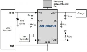
There are two: AOZ13984DI-02 and AOZ13987DI-02, both in 3 x 3mm thermally-enhanced DFN packaging, designed to be used in devices that are charged through a USB connector, to prevent current flowing back out of the device through the Vbus pin.
Inside is a control IC co-packaged with back-to-back mosfets, and reverse current under fault conditions can be blocked while working at up to 22V.
The primary differences are:
- AOZ13984DI-02: 33mΩ typical on-resistance, 5.5A continuous sink, 15A peak (10ms 2% duty)
- AOZ13987DI-02: 20mΩ typical on-resistance, 8A continuous sink, 20A peak (10ms 2% duty)
In both cases, normal operation is over 3.4 to 22V (28V abs max) and -40 to +125°C junction (thermal resistance is 2.8°C/W θjc and 36°C/W θja).
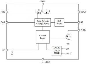 In the case of the 20mΩ AOZ13987, when the IC is enabled, it regulates Vout to be 35mV less than Vin from no-load, through medium load and up to the point that the mosfets saturate to 20mΩ. After this, the voltage across the mosfets is determined by load current. The 33mΩ AOZ13984 instead works on 70mV.
If for any reason Vout increases such that Vin – Vout is <35mV, it is assumed that current is about to be forced back through the IC and the gate driver forces the switch to turn off.
A fast comparator has been included to turn off the power switch if Vout has got more than 50mV higher than Vin.
“It is a two loop system,” AOS product director Peter Cheng told Electronics Weekly. “The fast comparator is the fail-safe feature if the Vout suddenly goes beyond Vin very fast – in under 10μs – and the ideal diode blocking is not fast enough to open the switch for protection.”
When the device is first enabled, or during auto-restart, the power switch is also kept off if Vout is 50mV higher than Vin, according to the data sheets. And the switch is turned off when the die reaches 140°C, after which it can only be re-enabled by either toggling the enable pin or cycling the input power supply.
Soft-on is implemented, so when device is enabled thorough its enable pin, the mosfet gates are controlled to ramp the output up linearly until Vout reaches Vin at a rate set by an external capacitor.